Carbon treatedAtomic Carbon coated cables and wires
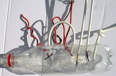
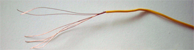
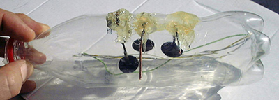
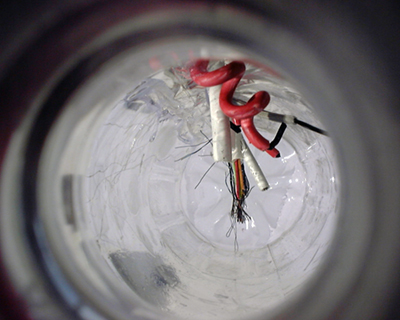
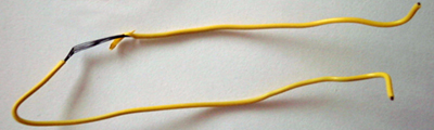
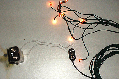
We have carried out several materials tests in our static reactors. One is the treatment of cables and wires that have copper strands inside their insulation coating. All copper wires and strands were still in their insulation sheath while being processed. Different types of cables and wires were introduced into or connected to plasma reactors. Some reactors were filled with some Kt Liquid, others only with pure plasma (a Kt Liquid vapor). No additional external energy sources - such as EUV from arcs, magnetic fields from solid magnets, electrical current, etc. - were used.
TWO KINDS OF TREATMENT
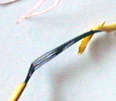
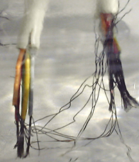
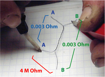
NEW INSULATING AND CONDUCTIVE PROPERTIESAlthough the strands are in direct contact, they are fully insulated from each other by the atomic carbon layers. This is proven in tests - at room temperature - with multi-meters and physical tests with batteries (9V) and lighting, where current was conducted through wires that were directly twisted round each other.
This means that a new proprietary type of wire has been developed, which can co-conduct several strengths of current at the same time through their different strands, and this will mean a revolution for all kinds of electric and electronic design. 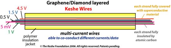 This approach can also be used for the design of transistors and integrated circuits. For example, surfaces with only a few atomic carbon layers – such as sp2 (Graphene) with ballistic conductive properties - can be mounted directly on each other while remaining insulated from each other. With techniques like etching special circuits can be made. Mr Keshe: "It is clear that we have found a number of new principles of atomic interactions and reaction on the atomic level, which were unknown till now. We developed methods of generating new processes in our reactors, and the coating of wires which are still in their insulation sheath is just one of the industrial applications we see. "When you are working at the atomic and nano level you are thinking in other sizes. Let’s say if the carbon atoms were the size of ping-pong balls then the insulation material - which we normally think of as being very close to the copper strands - could have gaps like tens of meters wide from the copper strands themselves, so the carbon atoms can travel easily through and be deposited on the free copper atoms which attract them. "Our method is that we mount full telephone cables in the wall of our reactors, leaving the rest of the cable outside the reactor, and the cables act like exhaust pipes to transport the atomic carbon while depositing them on the copper. This is a process at atomic level, not a chemical process, since the insulation of the wires is still intact. "We can apply this amazing wire treatment on the atomic and nano level immediately on an industrial scale. The process is quite simple. This new achievement confirms our previous findings that Carbon sp2 and sp3 can be deposited on various substrates and objects at room temperature and normal atmospheric pressure, without complicated systems like the traditional arcs treatment. We can provide industry with all kinds of nano-materials at very competitive prices." Of course the methods and applications are under patent pending, since they will change and simplify a large number of industrial processes, and this not only on the nano scale. Furthermore the original approach developed by Mr Keshe makes it possible to create self-sustaining energy systems that will lead to new kinds of electric generator. |