|
Graphene production
- Details
-
Category: Graphene production
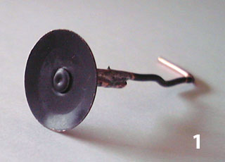 Cupper electrode with a layer of graphene Cupper electrode with a layer of graphene |
We have established a unique method of producing Carbon sp2, also called Graphene, in our static reactors. This happens at room temperature and in normal atmospheric conditions. The experiments, which are very quick and easy to perform, were repeated many times in several types of reactors. This is a major breakthrough since at present graphene is produced in complicated systems at temperatures of 700°-800°C.
|
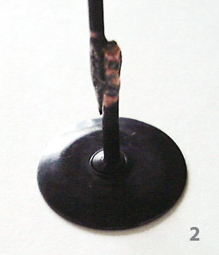 Cupper electrode with a layer of super conductive graphene Cupper electrode with a layer of super conductive graphene |
Raman Spectroscopy, performed by an independent laboratory, confirms sp2 of carbon on the copper electrode. This electrode shows several sp2 layers on top of each other. This is because we had previously used the tested sample for several different loadings and several carbon extractions from various materials. It was picked randomly from 30 or 40 pieces. The Raman Spectroscopy shows two main peaks in the graphs, one in the sp2 area and one in the sp3 area. The sp3 may indicate either that the weight of the upper layers has caused broken connections in the lower layers, or that the carbon layers on the electrode also contain some sp3, which are diamond-like deposits.
|
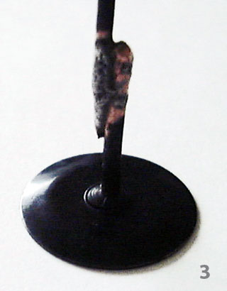 Cupper electrode with a layer of ballistic conductive graphene Cupper electrode with a layer of ballistic conductive graphene |
The disk of the sample has a diameter of 19 mm. In specially adapted reactors we are able to treat much larger surfaces of any shape and length, such as plates of 10 cm x 10 cm. The method can be applied for large scale production of nanofabric for new types of wafer for electronics, on a continuous base in industrial production lines. We believe that perfect nanofabrics of 500 microns (millionths of a meter) across are very feasible, and can be achieved very soon. By altering the exposure time in reactors we can attain the targeted number of sp2 layers of the required thickness. This process will be fine tuned in future tests with industrial partners.
|
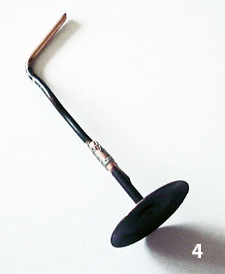 Cupper electrode with a layer of carbon sp2 graphene for FET transistors Cupper electrode with a layer of carbon sp2 graphene for FET transistors |
The first image shows minor damage on the outer side of the disk. This is caused by contact with desk surfaces. The samples coming out of a reactor don't have such damage. The blank spaces on the connection between the disk and the wire are caused by the solder material as the oil in it prevents deposition of carbon. The Raman test was not done on the sample shown on the images but with an identical sample.
|

The basic approach shown in the cola bottle reactor can easily be applied for large-scale industrial production. For example, we can design specific reactors to produce only sp3, thus to manufacture industrial diamond, transparent diamond and glassy carbon for various industrial applications. The presence of pure transparent diamond crystals on special electrodes was confirmed by experts in the Diamond Bourse of Antwerp. A project to produce transparent diamonds in dynamic reactors will be started.
In addition it is easy to produce boron nitrides, in mono-layers (a-BN). We can also treat various materials which are covered by insulation, such as telephone wires.
Already during tests in mid 2006 other properties were observed, such as porous C-structures which can be used for environmental cleaning. This is part of our IP. In April 2007 ESRF claimed the same discovery.
A similar system can be used for cleaning up CO2, NOx and SO2 from automotive, home and industrial exhaust gases. Adapted versions of these reactors can be used in water treatment systems to extract elements like Cadmium and Chromium. Also Trichloroethylene can be extracted from contaminated water in a simple way by using the electromagnetic fields in the plasma. TCE is widely found in drinking water, and California has some of the nation's worst contamination. (Article LA Times, 27 July 2006)
Please keep in mind that we consider the production of graphene as only one of the by-products of our plasma technology.
|